
LiveOPTICAL® and LiveFIB®
LiveOPTICAL® service launched, to compliment our secure LiveFIB® remote access FIB imaging.
LiveOPTICAL® video conferencing
LiveOPTICAL® remote project conferencing is the latest innovation from NanoScope. By extending our UNIQUE LiveFIB® capability to include OPTICAL MICROSCOPY and NANOMANIPULATION, NanoScope clients can now supervise all aspects of their projects, from the comfort of their own office.
By bringing together these complimentary microscopy techniques with real time project supervision, you can have the confidence to send your most valuable projects for actioning, while focusing on other important tasks. These powerful visual aids and on-line collaboration also have removed the need for you to travel to supervise these specialist interventions. Remote access FIB imaging and online collaboration also significantly reduces the documentation work required for each job and your travel costs.
Device Modification or Materials Analysis has never been greener or more cost effective.
Several conferencing software options support NanoScopes Live Microscopy options. Just click here to ask.

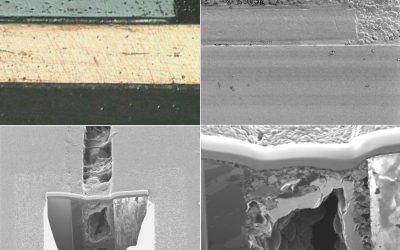
A magnified optical microscope image of a semiconductor device seen via a SKYPE user interface over the web.

An annotated FIB image of a semiconductor device during a via milling process seen via web link in a SKYPE user interface.
LiveFIB® – secure video conferencing during FIB interventions on your samples
NanoScopes UNIQUE LiveFIB® capability effectively puts a Focused Ion Beam microscope into the office of every engineer who needs one.
We offer secure remote access FIB imaging across all Ion Beam applications alongside real time consultation to accelerate the process and minimise the costs.
World class results without any instrument or expert engineer costs are available on an ‘as needed’ basis and without and training or lengthy preparation.
Log onto LiveFIB® and watch your problems get ionised.
Don't Be Shy. Get In Touch.
If you are interested in working together, send us an inquiry and we will get back to you straight away.
New Year – New Support – And we are off with a BANG
– helping you get to market with new IC designs and new packages and solving your yield, production or field return problems.
What’s your Sectional Preference?
Combining multiple sectioning methods with other techniques such as laser-assisted-wet-chemical-decapsulation and delayering techniques, can enable access to features buried deep within a complex chiplet or MCM packages.

IC Designers – Are you missing a trick?
A recent statistic from a well known design tool vendor showed that only 14% of new IC layouts were error free at 1st tape out. Hardly “right first time”.
Verification and modelling will only take you so far, especially for ASIC and Analog designs. High metal layer count, shrinking geometries, packaging developments and thermal issues aren’t helping either.