
FIB Services for Failure Analysts and Product Test Engineers
Electrical Micro-Probing – also to FIB deposited pads connected to buried nodes
Electrical micro-probing permits the driving or monitoring of a voltage or signal at any mid-circuit node(s) with or without available probe pads.
Our micro-probing facility with optical microscope permits direct electrical connection to structures down to 10×10 microns. This is sufficient to connect to power structures and any nodes connected to FIB deposited probe pads in a device.
We have a number of different probe types available or customers can repeat their own tips setup and test condition. Power supplies and a Tektronix curve tracer are on-site and available for your use to support your test protocol and confirm your FIB-layout edits and functionality changes are successful.
For a detailed description of the equipment and techniques available, go to the Tools and Techniques page.
There are 3 clear advantages
- It can be QUICK as it can be done directly on opened circuits without changing the device layout.
- IT WORKS ON PASSIVATED TOP LAYER TRACKS – by using FIB to open windows in the passivation coating.
- IT WORKS ON BURIED NODES –by first depositing a FIB probe pad on top of the passivation and connecting it down to the target node.


Don't be shy, get in touch.
If you are not sure about an aspect of this technique we’re happy to chat through it with you.
New Year – New Support – And we are off with a BANG
– helping you get to market with new IC designs and new packages and solving your yield, production or field return problems.
read more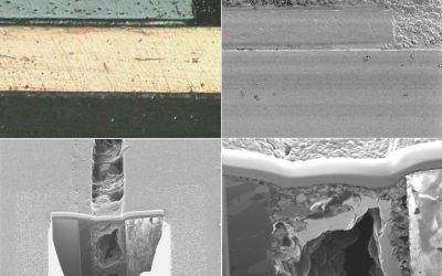
What’s your Sectional Preference?
Combining multiple sectioning methods with other techniques such as laser-assisted-wet-chemical-decapsulation and delayering techniques, can enable access to features buried deep within a complex chiplet or MCM packages.
read more
IC Designers – Are you missing a trick?
A recent statistic from a well known design tool vendor showed that only 14% of new IC layouts were error free at 1st tape out. Hardly “right first time”.
Verification and modelling will only take you so far, especially for ASIC and Analog designs. High metal layer count, shrinking geometries, packaging developments and thermal issues aren’t helping either.