
News & Articles
Keep up to date with all the latest NanoScope news and technical articles.
New Year – New Support – And we are off with a BANG
– helping you get to market with new IC designs and new packages and solving your yield, production or field return problems.
read more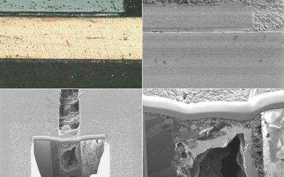
What’s your Sectional Preference?
Combining multiple sectioning methods with other techniques such as laser-assisted-wet-chemical-decapsulation and delayering techniques, can enable access to features buried deep within a complex chiplet or MCM packages.
read more
IC Designers – Are you missing a trick?
A recent statistic from a well known design tool vendor showed that only 14% of new IC layouts were error free at 1st tape out. Hardly “right first time”.
Verification and modelling will only take you so far, especially for ASIC and Analog designs. High metal layer count, shrinking geometries, packaging developments and thermal issues aren’t helping either.

Laser Assisted Decap of Plastic IC packages.
This has become a routine tool for IC Failure Analysis of Silicon and III/V devices, for FIB IC Nano-Surgery (FIB EDIT), and for Reverse Engineering for IP/Fake/Benchmarking check
read more
Are your Chips dying when you try to decap them?
IC Designers, Failure Analysts and Quality Assurance engineers have a common problem. They need to get into a fabricated IC while keeping it viable and testable.
read more
🚨 We’re exhibiting at Microelectronics UK 2025 this September!
🚨 We’re exhibiting at Microelectronics UK 2025 this September!
I hope to see you there- DM me now to book a 1 to 1 chat.
Lets talk about…
– FIB IC Nano-surgery for Chip designers to test and de-risk layout changes.
– Failure Analysis for Silicon, III/V’s, PCB’s and Modules, from boards to gates.
– Environmental/Reliability testing – with CSAM and FA support

Merry 3D X-ray X-mas from NanoScope Services
This X-ray map is of a 3 layer, FIB milled pattern in a 3 layer metal stack (Au, W and Al).
Our Xmas holiday is from 20th Dec to 6th Jan.
As 2024 draws to a close, we wish you a very Merry Christmas and a relaxing break.
For 2025 we hope that your Nano-structures are well formed, your FAB processes well qualified, that your designs are ‘right-first-time’ and failure-free, your packaging and PCBs are reliable and your joints well soldered

Merry Christmas 2023 – It’s been a Quality Year adding these exciting new Capabilities
Our big company NEWS is that we are now ISO 9001:2015 Certified
Our NEW microscope this year is a Sonoscan D24 Acoustic Microscope (large area CSAM).
Our New Technique this year is our Plasma FIB Capability.
We now offer ThermoFisher Hydra capabilities to our customers now including.
Lastly our new Sample Preparation Technique is Mechanical Grinding and Polishing.
Recent Comments