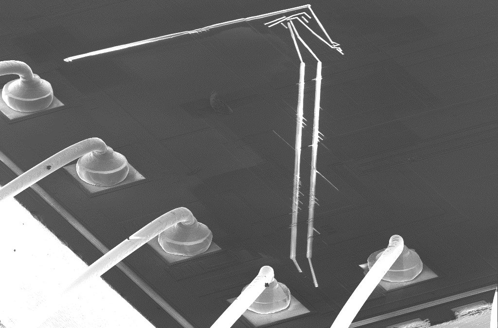
A recent statistic from a well known design tool vendor showed that only 14% of new IC layouts were error free at 1st tape out. Hardly “right first time”. Verification and modelling will only take you so far, especially for ASIC and Analog designs. High metal layer count, shrinking geometries, packaging developments and thermal issues aren’t helping either. BUT there is a tried and tested way of fixing 1st Silicon in just a few hours. It’s called FIB IC Nano-Surgery (historically called FIB Circuit Edit). For those unfamiliar with the technique, it uses a Focused Ion Beam microscope to physically cut and connect buried tracks on a fabricated IC, correcting layout errors in hours, and allowing you to test and verify a mask change BEFORE tape out. From a business perspective this effectively removes all the risk from such an expensive and time costly decision (new Silicon can take 3 months or more) at a time when a project delivery is at it’s most critical. Who wouldn’t choose to have working Silicon immediately for customer demos, chip, board and system level debug, and project support and investor confidence? HERES the danger – it used to be easy, but now it’s not. A decade ago anyone with a FIB or DualBeam in their lab could implement fixes with a high degree of confidence – but those days are long gone. Devices and packaging got more complex, and the FIB instruments themselves have evolved away from being optimised for Nano-Surgery as an application. So FIB Nano-Surgery has had to evolve, and the people doing it have had to become more specialised....
This has become a routine tool for IC Failure Analysis of Silicon and III/V devices, for FIB IC Nano-Surgery (FIB EDIT), and for Reverse Engineering for IP/Fake/Benchmarking checks. Copper bondwires, III/V die and shrinking package sizes have made it increasingly difficult to use an Acid-only approach to exposing part or all of a die surface. But you can’t just ablate all the plastic and expect the chip to still work, most laser wavelengths damage gates so it is still necessary to use wet chemistry under specific conditions for exposing the die surface....
I hope to see you there- DM me now to book a 1 to 1 chat. Lets talk about… – FIB IC Nano-surgery for Chip designers to test and de-risk layout changes. – Failure Analysis for Silicon, III/V’s, PCB’s and Modules, from boards to gates. – Environmental/Reliability testing – with CSAM and FA support. – FAB process qualifications – with nextday referenced metrology data. 📆 24 – 25 Sept | Excel London 🎯 www.microelectronicsuk.com 📍 Booth: H60 hashtag#MicroelectronicsUK hashtag#DeepTech hashtag#SemiconductorDesign Go to LinkedIn...
Closure times – NanoScope is closed from 20th December 2023 to the 5th January 2024 Our big company NEWS is that we are now ISO 9001:2015 Certified In our bid to improve our services on all fronts, we are very proud to have achieved ISO 9001 certification at the end of 2023 – more details to follow. We have already implemented our Quality Management System so you may spot these changes when you use us next. Our NEW microscope this year is a Sonoscan D24 Acoustic Microscope (large area CSAM). this state-of-the-art CSAM is already providing pre- and post- JEDEC Reliability checks for stress testing batches of devices (inc MSL testing) its providing checks for voids in complex planar sandwiches of materials – like polymers and metals it is also used as a Failure Analysis diagnostic tool for on-board packaging as a compliment to our X-ray capability. Our New Technique this year is our Plasma FIB Capability. We can offer ThermoFisher Hydra capabilities to our customers now including Xe for rapid milling of large sections – up to 100’s of μm in size/depth Ar for low kV polishing of (S)TEM sections and FEG SEM for high resolution imaging and Analysis in-situ. Lastly our new Sample Preparation Technique is Mechanical Grinding and Polishing. As boards and modules get smaller and more complex, the boundary between substrate and die requires more advanced investigation, so the need for accurate mechanical sectioning as a starting point for any structural analysis becomes increasingly important. Good Mechanical prep is more often the starting point for a Plasma or Gallium FIB section. (Section of a Section...
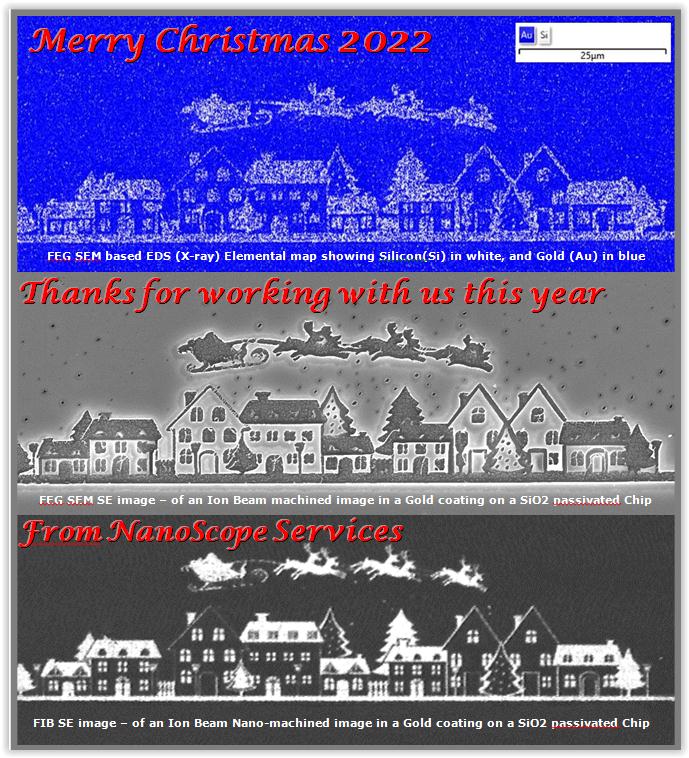
Merry Christmas – Nano-fun for the end of year 2022 Wishing all friends of our small team, the very best for the festive season, and a prosperous start to...
There are many advantages of correcting an IC design with FIB Nano-Surgery, but sometimes there are also problems, and many designers have been put off the technique. Did your last FIB work as you expected? Or was the yield low? or you got results you couldn’t explain? A quick recap of the reasons to do a FIB edit and how you would go about it, might be helpful. SCENE: So you’ve taped out your big new design, and 4 months and ₤400,000 /$/€ later, your 1st Silicon devices have arrived for tests to start. And immediately, there’s a problem. If you are lucky, then a normal functional test has failed and after a few days of head scratching it becomes clear what the cause is, and what the most likely metal fix should be. If you are unlucky and it’s more subtle, but still a show stopper for customer acceptance, then the fix strategy may be less obvious. Either way, prompt action is required and there are some difficult decisions to make. Your colleagues, customers and suppliers are all waiting to help get your product to market. Then there is the expense and the delays: to testing, to qualification, to sales and to revenue – which all add up to a serious commercial inconvenience. What ARE your options here? Risk a design change because there is a high confidence that the fix is understood? Do you roll the dice (the expensive and time consuming ones) and trust that the fix will work? Or spend a week trying to get a few chips fixed using FIB nano-surgery and give yourself some...


Recent Comments