
Your 1st Silicon Emergency Service
For FABLESS design houses we offer FIB CIRCUIT EDIT services for rapid verification and electrical debug of 1st Silicon.
FIB Circuit Edit Service for Chip Designers and Layout Engineers
FIB circuit edit – for when your 1st Silicon needs a mask change before volume production.
When “1st time right” is not right, choosing the best partner for FIB IC Nano-Surgery is a critical decision for a design manager. It is important to know who you can trust to quickly help you mitigate the serious technical and commercial disruption to your NPI process, and the pitfalls to avoid.
You need to know –
Can I have working devices in a few hours or days? – NanoScope specialises in the fastest turnaround times in the Europe and Middle East time zones.
What’s my Yield going to be? – Our world-beating better than 95% 1st time success rate has been standard since we opened in 2006, and we’ve been doing this longer than anybody – since 1992. For the most complex fixes we offer yield predictions BEFORE you commit, based on 28+ years of experience.
How can I reduce the risks? – NanoScope offers free consultation on all projects, we work directly with your designers to maximise the fix yield, and reduce the time needed for any fix BEFORE we quote.
What if the intervention doesn’t fix the problem? – 30% of all fixes specified by designers do not fix the correct electrical problem found. BUT a wrong fix correctly implemented proves that a different metal fix is required – this saves an entire metal fix FAB run, and helps you understand the REAL problem more quickly.
I’ve had bad results/low yield before, why are you different? – We are FIB technologists and we specialise in Semiconductor device Nano-Surgery. These are specific skills required for delivering the best advice and the highest yields. Respect the complexity of the process, and choose your partner based on what they need to know.
Are you value for money? – Do you choose a FIB partner based on their hourly rate? Or for convenience? (using the FA lab at your Test house or Reliability partner). Maybe you use a University with a new FIB-SEM? (the wrong tool). If the operator was trained by a vendor (limited knowledge), or mostly does Failure Analysis (the wrong application), or research (unrelated), or they are just cheap (why?), what value can they add in reality?
Getting you the right fix for the right problem in the shortest time is how we add value to your business.

FIB Circuit Edit: Full process flow
First – Check the structure
Sometimes information is limited, but the device construction defines how we can modify it. We use non-destructive X-ray and/or CSAM to understand the lead frame design, die attach/stacking/size/position/orientation, bondwire type and layout etc. to optimise your opening strategy.
Second – Open the device – economically, while leaving it fully functional
The die surface must be open at the point of intervention(s), giving sufficient access, a clean surface, and without compromising how the device will be tested AFTER the intervention is complete. These steps are defined by 4 things
- Structure and materials – There are different approaches for Ceramic, Metal, Hybrid, Plastic, Eco Plastic, Chip and Wire, Globtop, Embedded etc. The Bond wires (and other metal structures) can be sensitive to acid and sometimes a laser pre-cavitation step first. Ceramics and Metal cans need mechanical processing. Conformal coatings and solder masks, glob topping and other protections all have different requirements.
- Intervention requirements – How much access do we need? are the new FIB tracks long (mm’s) or local (μm’s). Does the fix require maximum gas flux? Closer nozzle approach needs more room. If multiple sites need modification then a full decap may be the best approach.
- Post fix testing requirements – how will the device be tested AFTER nano-surgery. If you’re using a socket, then preserving the lid for clamping is essential for easy testing. If you’re re-flowing the chip, it may need resealing to protect the fix. WLCSP has different issues again.
- Re-sealing – refilling an opening is sometimes required, and materials vary in quality, reactivity, cost and curing time.
Third – Optimise the Fix for best results
Chip designers are not FIB technologists and they don’t construct chips. The limitations and capabilities of FIB plus the nano-surgery process and how to optimise it, plus knowing the structure and behaviour of the materials to be modified, are all required for a successful fix. The final version after the FIB circuit edit should yield well, and be economic to implement.
By working with your designers we can advise how to achieve this result. Changing the location, target layers and routes of the FIB operations by just a few microns, can change an intervention yield by 100% and the costs too.
Fourth – Implement the Fix
Processing the devices with the correct ESD handling protocols, mounting , grounding, FIB work, cleaning, inspection (pre- and post), shipping and support in the shortest time frame.
The fix must also survive the testing process. If the device is to be heated – then standard Platinum depositions will not survive (it’s only 14% Pt and 86% Hydrocarbon), and solder can short out FIB fixes if not properly protected.
Fifth – Results review and remedial actions
Confirming intervention success and quickly completing remedial actions or rework are as important as delivering devices on time. If alternative fixes are necessary, these are often needed more rapidly than before. This are all part of a successful process and how NanoScope’s FIB circuit edit service ensures you have working devices in a few hours or days, with our >95% success rate.


Don't Be Shy. Get In Touch.
If you are interested in working together, send us an inquiry and we will get back to you straight away.
New Year – New Support – And we are off with a BANG
– helping you get to market with new IC designs and new packages and solving your yield, production or field return problems.
read more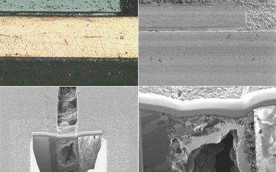
What’s your Sectional Preference?
Combining multiple sectioning methods with other techniques such as laser-assisted-wet-chemical-decapsulation and delayering techniques, can enable access to features buried deep within a complex chiplet or MCM packages.
read more
IC Designers – Are you missing a trick?
A recent statistic from a well known design tool vendor showed that only 14% of new IC layouts were error free at 1st tape out. Hardly “right first time”.
Verification and modelling will only take you so far, especially for ASIC and Analog designs. High metal layer count, shrinking geometries, packaging developments and thermal issues aren’t helping either.

Laser Assisted Decap of Plastic IC packages.
This has become a routine tool for IC Failure Analysis of Silicon and III/V devices, for FIB IC Nano-Surgery (FIB EDIT), and for Reverse Engineering for IP/Fake/Benchmarking check
read more
Are your Chips dying when you try to decap them?
IC Designers, Failure Analysts and Quality Assurance engineers have a common problem. They need to get into a fabricated IC while keeping it viable and testable.
read more
🚨 We’re exhibiting at Microelectronics UK 2025 this September!
🚨 We’re exhibiting at Microelectronics UK 2025 this September!
I hope to see you there- DM me now to book a 1 to 1 chat.
Lets talk about…
– FIB IC Nano-surgery for Chip designers to test and de-risk layout changes.
– Failure Analysis for Silicon, III/V’s, PCB’s and Modules, from boards to gates.
– Environmental/Reliability testing – with CSAM and FA support