
'QwikQual'
Chip makers, QwikQual wafer process qualification gets your production ramped up or helps correct a yield excursion.
Services for Chip Makers and FAB Product Engineers.
‘QwikQual’ wafer process qualification can help get your production ramped up, or speed up the solving of a yield excursion in your process.
Sometimes you need to know what your process tool is achieving at a specific location which is critical to your final yield, and so we have introduced a rapid instrument qualification process for FAB engineers, who need site-specific process data on a sameday/next day basis.
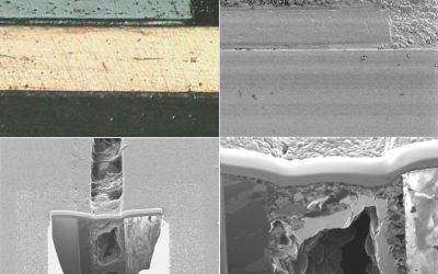
Our ‘QwikQual’ service is for 1 or 2 micro cross-sections with imaging and calibrated metrology taken from a specific location to help you independently qualify your manufacturing equipment – specifically for clients who have pre-registered for this service.
We will email the images directly to you as they are produced, allowing you to make quick decisions for your production line and your process.
This service is ideal for semiconductor foundries who are ‘ramping up’ a new process or for supplying site-specific customer qualification data. Our wafer process qualification can also supply precise information for non-standard Quals.

It’s got to be
- FAST
- Independent
- From the right location
- Correct (Accurate)
- Referenced to traceable standards
- Reasonably priced
How do I do that?
- BEFORE – Sign up to ‘QwikQual’ wafer process qualification service
- TODAY – Ship the sample to us to arrive just after 8am – not before (or before 5pm for next day work) – do this first – 2 sections max
- Call us for taxi or bike courier contacts
- TODAY – Email us your sectioning job instructions (guidelines on website) and telephone us to advise that there is a project arriving.
- TOMORROW – We run the job before ‘start of day’
- TOMORROW – results emailed to you before 10AM
- PO – draw down to agreed limit
- You can watch over the web with ‘LiveFIB’ if needed.
Don't Be Shy. Get In Touch.
If you are interested in working together, send us an inquiry and we will get back to you straight away.
What’s your Sectional Preference?
Combining multiple sectioning methods with other techniques such as laser-assisted-wet-chemical-decapsulation and delayering techniques, can enable access to features buried deep within a complex chiplet or MCM packages.

IC Designers – Are you missing a trick?
A recent statistic from a well known design tool vendor showed that only 14% of new IC layouts were error free at 1st tape out. Hardly “right first time”.
Verification and modelling will only take you so far, especially for ASIC and Analog designs. High metal layer count, shrinking geometries, packaging developments and thermal issues aren’t helping either.

Laser Assisted Decap of Plastic IC packages.
This has become a routine tool for IC Failure Analysis of Silicon and III/V devices, for FIB IC Nano-Surgery (FIB EDIT), and for Reverse Engineering for IP/Fake/Benchmarking check