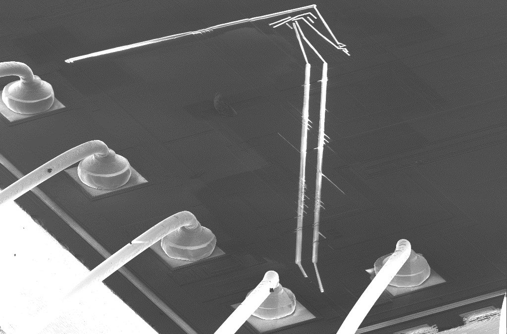
There are many advantages of correcting an IC design with FIB Nano-Surgery, but sometimes there are also problems, and many designers have been put off the technique. Did your last FIB work as you expected? Or was the yield low? or you got results you couldn’t explain? A quick recap of the reasons to do a FIB edit and how you would go about it, might be helpful. SCENE: So you’ve taped out your big new design, and 4 months and ₤400,000 /$/€ later, your 1st Silicon devices have arrived for tests to start. And immediately, there’s a problem. If you are lucky, then a normal functional test has failed and after a few days of head scratching it becomes clear what the cause is, and what the most likely metal fix should be. If you are unlucky and it’s more subtle, but still a show stopper for customer acceptance, then the fix strategy may be less obvious. Either way, prompt action is required and there are some difficult decisions to make. Your colleagues, customers and suppliers are all waiting to help get your product to market. Then there is the expense and the delays: to testing, to qualification, to sales and to revenue – which all add up to a serious commercial inconvenience. What ARE your options here? Risk a design change because there is a high confidence that the fix is understood? Do you roll the dice (the expensive and time consuming ones) and trust that the fix will work? Or spend a week trying to get a few chips fixed using FIB nano-surgery and give yourself some...

Recent Comments