– helping you get to market with new IC designs and new packages and solving your yield, production or field return problems. Take 30 seconds to review your extended toolkit for comprehensive, logic to power, fast-turn, gate-to-board issues. 1) FIB IC Nano-surgery to pre-test your metal fix without the risk. 2) Failure Analysis for Silicon and Compound devices, Chiplets and PCB’s. 3) Reliability testing for packages (HAST,THB,PreCon etc.) with onsite CSAM. 4) RevEng for Technology reviews from 7nm’s up to Power modules. 5) 24hr Si and III/V FAB process Quals 6) Nano-Materials imaging and analysis ...
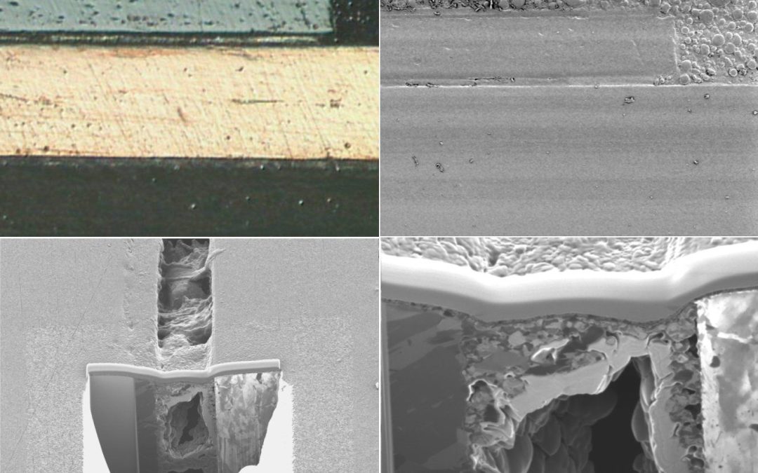
In micro-electronics if you get it wrong, your data will be wrong. Whether you are qualifying a fabrication process, or analysing a structure or a failure, on everything from Soldered PCB’s down to IC FINFETS, you need the right type of X-section. Each type comes with its benefits and limitations, and as devices and packaging shrinks and gets more sophisticated, using the right approach defines your success rate. What is becoming more and more useful is the ability to use MORE THAN ONE of these techniques at the same time. To do that you have to have a partner who understands your technology and has expertise in all of them. And Sectioning is not done in isolation. Combining multiple sectioning methods with other techniques such as laser-assisted-wet-chemical-decapsulation and delayering techniques, can enable access to features buried deep within a complex chiplet or MCM packages. I’ll go into more detail in future posts, but here’s a quick overview of your sectioning choices. Mechanical sections – used for cutting through larger structures like Solder, PCB’s, SMT’s and IC’s. These can be done with 2D or 3D embedding and polishing, but can suffer from soft materials smearing and vibration artefact during sampling. They can be improved and enhanced with various types of Ion Beam post-processing, from BiB to FIB. Plasma FIB Sections – features up to a few hundred microns is size. No smearing or cracking, but prone to surface damage, localised heating and Ion Beam curtaining when used on complex materials systems. Ga+FIB Sections – features less than 100 microns in size. Negligible surface damage, no heating or curtaining, and can...

Recent Comments