– helping you get to market with new IC designs and new packages and solving your yield, production or field return problems. Take 30 seconds to review your extended toolkit for comprehensive, logic to power, fast-turn, gate-to-board issues. 1) FIB IC Nano-surgery to pre-test your metal fix without the risk. 2) Failure Analysis for Silicon and Compound devices, Chiplets and PCB’s. 3) Reliability testing for packages (HAST,THB,PreCon etc.) with onsite CSAM. 4) RevEng for Technology reviews from 7nm’s up to Power modules. 5) 24hr Si and III/V FAB process Quals 6) Nano-Materials imaging and analysis ...
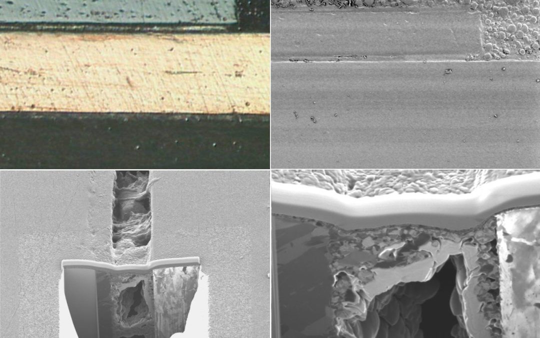
In micro-electronics if you get it wrong, your data will be wrong. Whether you are qualifying a fabrication process, or analysing a structure or a failure, on everything from Soldered PCB’s down to IC FINFETS, you need the right type of X-section. Each type comes with its benefits and limitations, and as devices and packaging shrinks and gets more sophisticated, using the right approach defines your success rate. What is becoming more and more useful is the ability to use MORE THAN ONE of these techniques at the same time. To do that you have to have a partner who understands your technology and has expertise in all of them. And Sectioning is not done in isolation. Combining multiple sectioning methods with other techniques such as laser-assisted-wet-chemical-decapsulation and delayering techniques, can enable access to features buried deep within a complex chiplet or MCM packages. I’ll go into more detail in future posts, but here’s a quick overview of your sectioning choices. Mechanical sections – used for cutting through larger structures like Solder, PCB’s, SMT’s and IC’s. These can be done with 2D or 3D embedding and polishing, but can suffer from soft materials smearing and vibration artefact during sampling. They can be improved and enhanced with various types of Ion Beam post-processing, from BiB to FIB. Plasma FIB Sections – features up to a few hundred microns is size. No smearing or cracking, but prone to surface damage, localised heating and Ion Beam curtaining when used on complex materials systems. Ga+FIB Sections – features less than 100 microns in size. Negligible surface damage, no heating or curtaining, and can...
A recent statistic from a well known design tool vendor showed that only 14% of new IC layouts were error free at 1st tape out. Hardly “right first time”. Verification and modelling will only take you so far, especially for ASIC and Analog designs. High metal layer count, shrinking geometries, packaging developments and thermal issues aren’t helping either. BUT there is a tried and tested way of fixing 1st Silicon in just a few hours. It’s called FIB IC Nano-Surgery (historically called FIB Circuit Edit). For those unfamiliar with the technique, it uses a Focused Ion Beam microscope to physically cut and connect buried tracks on a fabricated IC, correcting layout errors in hours, and allowing you to test and verify a mask change BEFORE tape out. From a business perspective this effectively removes all the risk from such an expensive and time costly decision (new Silicon can take 3 months or more) at a time when a project delivery is at it’s most critical. Who wouldn’t choose to have working Silicon immediately for customer demos, chip, board and system level debug, and project support and investor confidence? HERES the danger – it used to be easy, but now it’s not. A decade ago anyone with a FIB or DualBeam in their lab could implement fixes with a high degree of confidence – but those days are long gone. Devices and packaging got more complex, and the FIB instruments themselves have evolved away from being optimised for Nano-Surgery as an application. So FIB Nano-Surgery has had to evolve, and the people doing it have had to become more specialised....
This has become a routine tool for IC Failure Analysis of Silicon and III/V devices, for FIB IC Nano-Surgery (FIB EDIT), and for Reverse Engineering for IP/Fake/Benchmarking checks. Copper bondwires, III/V die and shrinking package sizes have made it increasingly difficult to use an Acid-only approach to exposing part or all of a die surface. But you can’t just ablate all the plastic and expect the chip to still work, most laser wavelengths damage gates so it is still necessary to use wet chemistry under specific conditions for exposing the die surface....
IC Designers, Failure Analysts and Quality Assurance engineers have a common problem. They need to get into a fabricated IC while keeping it viable and testable. Applications like FIB Nano-surgery, fault localisation by Thermal/Emission imaging or electrical micro-probing, all need the device to function after the Silicon is exposed. This means Decapsulation using Acid is more important than ever, but it’s becoming increasingly difficult with shrinking package sizes and Copper bondwires. Old school Jetetch machines just haven’t kept up. Each lab that offers this has its own unique and hard-won recipes. Ours uses different mixtures of fuming acids, digesters and solvents to clear and clean the die surface without compromising the die attach, bonding, bumps or lead frame. We also vary the temperature to preserve delicate structures and apply Ultrasound too. This all happens AFTER the pre-cavity laser step detailed in my previous post on this topic. This short clip shows the wet chemistry and ultrasonic steps needed to open the full surface of a die (confidential-pixelated), but even this is not the full story. How are you going to test it? Or power it up for imaging the failure mode? Soldering an open device to a test board carries risks from solder and flux damage, and the high temperatures also damage FIB modified devices with a low quality metal deposition (Pt). The simple answer is to use a socket, but can you still image the die surface once it is closed? And if you have remove the top of the package, will it still fit and make good contact? Partial decaps, or chip-and-wire type PCB mounting are straight...
I hope to see you there- DM me now to book a 1 to 1 chat. Lets talk about… – FIB IC Nano-surgery for Chip designers to test and de-risk layout changes. – Failure Analysis for Silicon, III/V’s, PCB’s and Modules, from boards to gates. – Environmental/Reliability testing – with CSAM and FA support. – FAB process qualifications – with nextday referenced metrology data. 📆 24 – 25 Sept | Excel London 🎯 www.microelectronicsuk.com 📍 Booth: H60 hashtag#MicroelectronicsUK hashtag#DeepTech hashtag#SemiconductorDesign Go to LinkedIn...


Recent Comments