
 In micro-electronics if you get it wrong, your data will be wrong.
Whether you are qualifying a fabrication process, or analysing a structure or a failure, on everything from Soldered PCB’s down to IC FINFETS, you need the right type of X-section.
Each type comes with its benefits and limitations, and as devices and packaging shrinks and gets more sophisticated, using the right approach defines your success rate.
What is becoming more and more useful is the ability to use MORE THAN ONE of these techniques at the same time.
To do that you have to have a partner who understands your technology and has expertise in all of them.
And Sectioning is not done in isolation.
Combining multiple sectioning methods with other techniques such as laser-assisted-wet-chemical-decapsulation and delayering techniques, can enable access to features buried deep within a complex chiplet or MCM packages.
I’ll go into more detail in future posts, but here’s a quick overview of your sectioning choices.
Mechanical sections – used for cutting through larger structures like Solder, PCB’s, SMT’s and IC’s.
These can be done with 2D or 3D embedding and polishing, but can suffer from soft materials smearing and vibration artefact during sampling.
They can be improved and enhanced with various types of Ion Beam post-processing, from BiB to FIB.
Plasma FIB Sections – features up to a few hundred microns is size. No smearing or cracking, but prone to surface damage, localised heating and Ion Beam curtaining when used on complex materials systems.
Ga+FIB Sections – features less than 100 microns in size. Negligible surface damage, no heating or curtaining, and can use protection from FIB/SEM deposited materials straps.
Thinned FIB sections – or (S)TEM sections. For targets less than 20 microns in size, and for imaging resolution down to the crystal lattice.
For various applications these can be left in-situ, or nano-extracted to a TEM grid inside the instrument, or on the bench. No surface damage or curtaining under normal conditions.
At NanoScope Services Ltd we specialise in all of the above, and in combining these techniques to provide a higher level of detail.
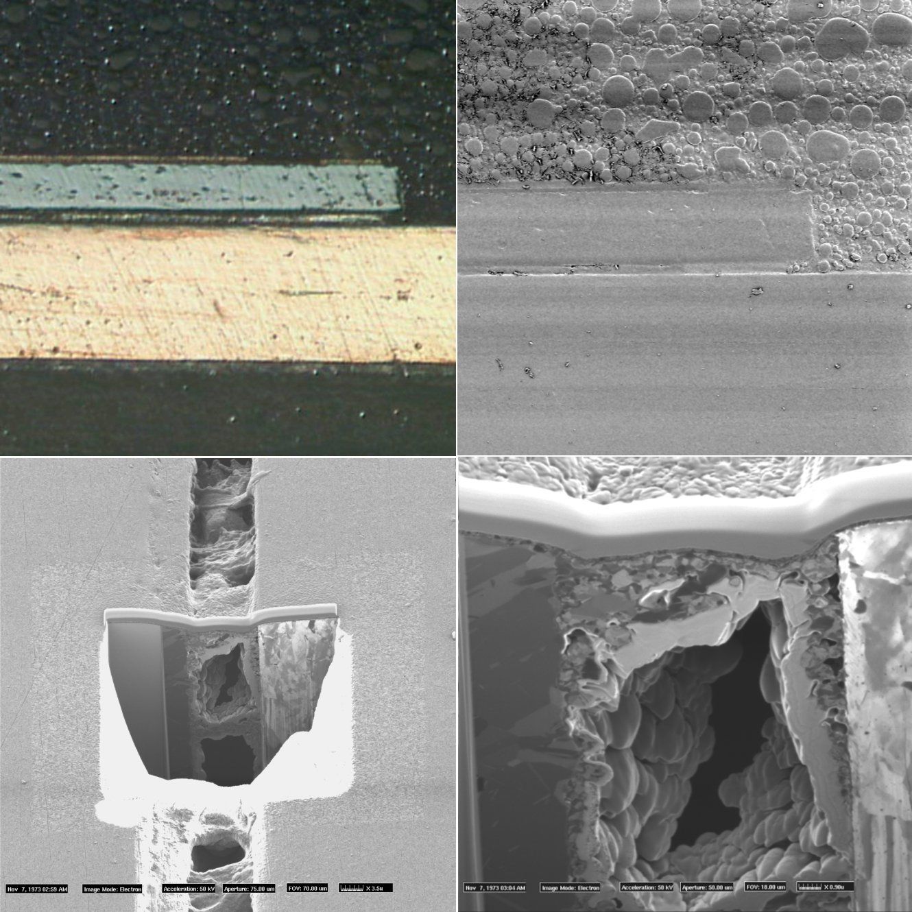
Here you can see an example of how a soldered semiconductor device has been Mechanically X-sectioned, imaged by Optical microscope, Au coated and imaged by FIB-SEM, and then FIB Sectioned to show the real issues present at the solder interface.
We call this “Section of a Section”. There is ZERO artefact below the surface, strong materials and metal grain contrast, and exact failure site placement.
The enhanced versatility of using multiple techniques together, enables native state data to be accessed within complex 3D structures.
Thanks to CML Micro and Jo Gibbins for permission to use the images, and shout outs to Antony Moor and Wayne Lam, PhD for the wider collaboration.
Please DM me here with questions or comments.
hashtagmicroelectronics hashtagfailureanalysis
Recent Comments