Our latest newsletter covers: New Services complement our Inspection and Analysis Options New AFM capability for rapid turn high resolution surface analysis High-resolution thermal imaging of chips and ICs – a great complement to our existing nano-surgery services X-Ray imaging for detailed inspection of a device’s internal structure and connections Acoustic Microscopy (CSAM) for detailed before/after checks. Download it here – E-Newsletter Summer...
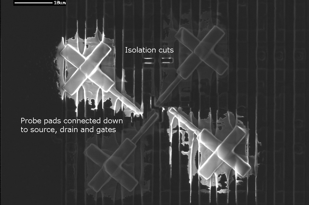
Download here : FIB assisted electrical debug- June 2018 FIB assisted electrical debug (micro-probing your layout) for 1st Silicon (part of the NanoScope ‘Summer of Love’ rel1.1- 28 June 2018) An often overlooked option in the race to get 1st Silicon devices working, is simple electrical probing (µm), but why is this? Well the reasons are all very human. We think because line-widths are getting smaller and top down access to (often) buried nodes is almost impossible (for anything that’s not top layer metal), that this technique is simply not applicable now. So the questions and options we consider run along these lines “How can I get through a WL-CSP package (for example) and get a needle onto a buried node to find the state of that node? Impossible, right? And the track is only 90nm’s wide anyway, so the probing station I will need will not only be extremely expensive to buy/rent/use, but could be far away, meaning I’ll have to travel and possibly spend a couple of days trying to get that to work. And even if everything goes well, it’s likely it won’t give me a clean contact and a clear answer which will be difficult to explain, even if I can get a needle down without breaking the circuit right away. And I’ll have to explain and justify this whole risky process to the project leader who’s not going to like it when I come back with half an answer, a big invoice to go with it and 2 weeks lost as well.” So instead of all that pain, it’s quite human of us...
Dear LinkedIN and NanoScope contacts – New and Old Firstly – thanks for being connected – If you are, then we share a mutual interest in a technical area where I, and my company NanoScope Services, are active. It could be FIB Circuit nano-surgery, Microscopes and accessories, FIB applications development, Failure Analysis, or even Marketing. But it could even be low cost qualification of automotive parts for space applications – so a diverse Nano-bag of outsourced R&D support, but all linked to advanced FIB Nano-engineering. I think LinkedIN is a great format for sharing updates – but I am terrible at this, and I need to improve. So… after several years of complete silence (hey, we’ve been busy…), it’s time again to reach out and renew those contacts and friendships from so many projects and collaborations. Over the next couple of months I’m going to post some LinkedIN articles about new techniques and capabilities – and how they can add value, and maybe how we can too. (check out some previews here, here, here and here if you are the impatient type) I can promise these feeds will have all the attributes I myself value in a message – they will be OCCASIONAL, SHORT, INFORMED, HELPFUL, NOT TOO SERIOUS and FREE (with a cool picture). Please comment if the urge takes you – good or bad, it’s all good, especially if it’s about something we don’t do yet, or something we can do better. Let’s start a conversation this Summer. With kind regards,...
Press release 10th March 2015 Every two years Admati Agency hosts an ‘invite only’ technical seminar for their growing customer base and some new invitees in Israel. The seminar provides a forum for introducing the latest developments from the firms represented by Admati and also to introduce the capabilities of the latest companies to join the group since the last meeting. NanoScope partnered with Admati in 2014 and this year we will present our Semiconductor and high tech support services at this seminar for the first time. This year the seminar will be held on the 28-April-2015 at the Tel Aviv Hilton. We will be presenting our capabilities for advanced FIB (Focused Ion Beam) IC circuit nano-surgery, single node Failure Analysis with comprehensive de-capsulation capabilities, rapid Fab process qualifications and advanced microscopy for small geometries and materials analysis. Other companies presenting will be: Intel – Case study presentation Reltech – Independent Reliability testing services Phasix ESD – Independent ESD testing services Special guest speaker (to be announced) ThermoFisher Scientific, Interconnect Devices (IDI) and others to be confirmed. A more detailed agenda will be released nearer the date to registrants. Representatives from 17 major Israeli semiconductor companies are registered to attend and we expect several more over the coming weeks. If you are interested to learn more about the meeting please contact us here. Request a LinkedIN invite here. Go to the NanoScope website here. Telephone +44 (0)1179576225 Send an email here. Contact : Lloyd Peto NanoScope Services Ltd. No30 Station Road Workshops Kingswood Bristol BS15 4PJ,...



Recent Comments