NanoScope gave an Online invited Tutorial on behalf of IMAPS UK on the 18th September 2020 on the subject of Focused Ion Beam (FIB) Circuit Nano-Surgery and Failure Analysis from Board to Gate. The Tutorial Archives can be accessed here. This presentation included a comparison of Cross Sectioning techniques with a comparison of the benefits and limitations of each method. Conventional Mechanical sectioning (with extended capabilities) vs FIB micro-sectioning vs Plasma FIB Sectioning. Also included was an introduction to the techniques of Silicon IC Circuit Nano-Surgery and other IC specific techniques that are now becoming possible to perform on package substrates, system boards, complex packages and other novel die mounting...
Dear LinkedIN 1 st contacts and NanoScope Customers Why not try something new while you are working from home, and Video inspect your own IC design live over the web? As our normal activities are curtailed by Covid19, we have to positively look out for new ways of doing things. This especially requires a much heavier use of video conferencing and getting used to that as well. Working and socialising remotely like this gives us the chance to adapt and innovate quickly, and is more necessary in order to maintain our morale, and our professional momentum. If we are successful in this, we will be able to minimise the disruption to our lives and to our companies, and reduce the time needed to get back to normal afterwards. Trying something new may even teach us some valuable lessons about what is important, and how to improve ourselves and our processes. So why not give this a go, and join us on-line. What can I see? This offer is for our LiveOPTICAL capability, and so permits the full imaging capabilities that our optical microscopes permit. This uses white light and is capable of magnifications of up to 1000X. We can navigate around your device with your direction and change imaging conditions and light incidence to highlight specific information as you wish. You can review chip ID’s and bonding layout, type, alignment & integrity (useful anti-counterfeit checks). You can see what that external IP block looks like, and where it connects to your design. You can confirm the presence of contamination, or suspected defects or mask errors. Check RDL metal and...
Let’s carefully collaborate our way through the ongoing Covid 19 crisis, and help drive the post pandemic recovery and growth. Luckily we were already set up for working with you remotely, so we can seamlessly support your new designs/products or analysis so that you can to be ready, and your projects still on time. To adapt to the new reality of Covid19, there has had to be a few subtle changes to the way we operate – but it’s all very sensible. We have adapted our protocols to operate normally while protecting our own staff (even from each other) Our Couriers are still running so sending and receiving devices/boards/samples is still normal. Our free project consultancy is unchanged via telephone and via video conferencing. We have upgraded the bandwidth and refresh times of our LiveFIB and LiveOPTICAL remote consultancy/microscopy options – you can still visit to supervise your work being done – but now ‘virtually’. This also saves non-urgent travel risks and costs. Sample handling is always done in sterile conditions, and return shipping is in sterile packaging. For you this means No new risks for you for handling, shipping, discussing and supervising external projects. No new project delays, lower costs (no travel), less time needed for documentation (virtual meetings), same rapid project turnaround, same professional – confidential – expert service. Extremely low exchange rates – so if you pay in Dollars or Euro’s, you have a historically lower cost. So even if you are now working from home, and things could be better – Better call NanoScope Lloyd.Peto@NanoScopeServices.com +44(0)7768...
Dear EU contacts and customers, As the UK general ‘Brexit’ Election gets underway – we invite all our EU customers to VOTE AS WELL. NanoScope have voted to boost the Euro exchange rate again. So now until Brexit is settled your 1€ spent will buy your ₤1 of support for your Semiconductor Design FIB-Nanosurgery, Nano-tech development or Failure Analysis project. With a record low Euro to GBP exchange rate – there is already a smart advantage to placing your project with us in the UK, and with this offer you can vote for an extra 19% cost reduction (exchange rate buy Euros 29/11/2019). Click here to get a quote NanoScope Services – your European FIB IC Nano-surgery Lab ...
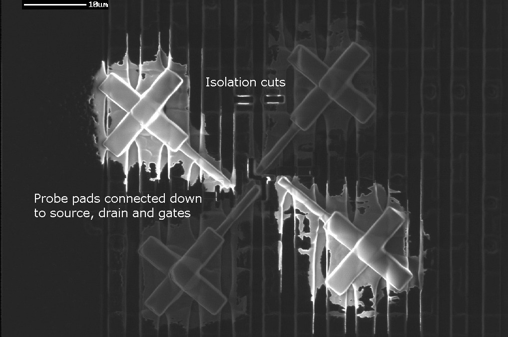
Download here : FIB assisted electrical debug- June 2018 FIB assisted electrical debug (micro-probing your layout) for 1st Silicon (part of the NanoScope ‘Summer of Love’ rel1.1- 28 June 2018) An often overlooked option in the race to get 1st Silicon devices working, is simple electrical probing (µm), but why is this? Well the reasons are all very human. We think because line-widths are getting smaller and top down access to (often) buried nodes is almost impossible (for anything that’s not top layer metal), that this technique is simply not applicable now. So the questions and options we consider run along these lines “How can I get through a WL-CSP package (for example) and get a needle onto a buried node to find the state of that node? Impossible, right? And the track is only 90nm’s wide anyway, so the probing station I will need will not only be extremely expensive to buy/rent/use, but could be far away, meaning I’ll have to travel and possibly spend a couple of days trying to get that to work. And even if everything goes well, it’s likely it won’t give me a clean contact and a clear answer which will be difficult to explain, even if I can get a needle down without breaking the circuit right away. And I’ll have to explain and justify this whole risky process to the project leader who’s not going to like it when I come back with half an answer, a big invoice to go with it and 2 weeks lost as well.” So instead of all that pain, it’s quite human of us...


Recent Comments